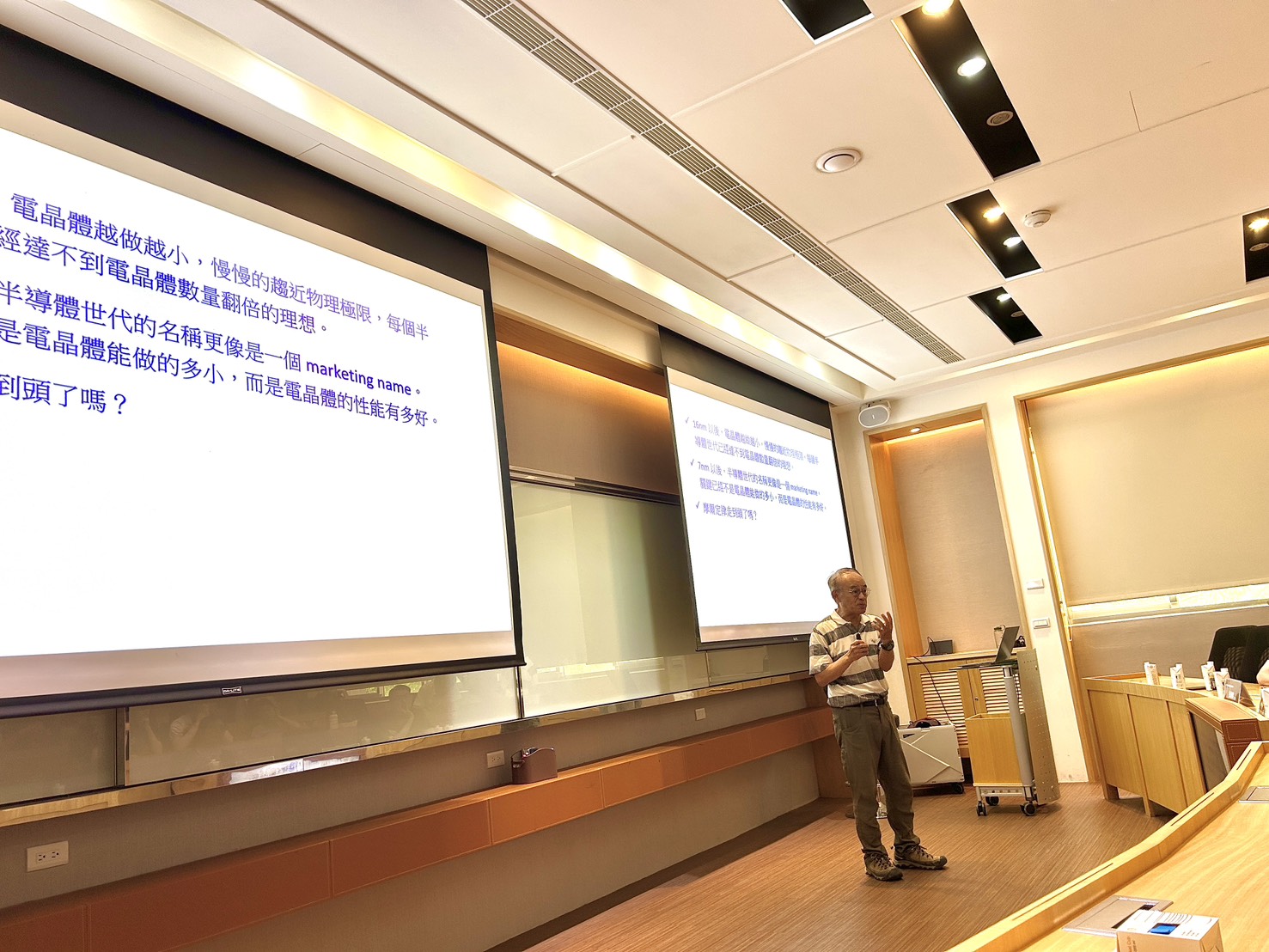
The Center for Business Sustainability at National Chengchi University (NCCU) hosted an open lecture titled "The Birth of a Chip: Telling the Story to Those Outside the Industry" (一個晶片的誕生 — 給不是這行的人說故事) on May 22, 2026, at Room 260201, NCCU College of Commerce. The speaker was Dr. Chip Peng (彭健雄), a materials science engineer with over 30 years of semiconductor industry experience and former Director of Foundry Operations at NVIDIA.
Designed expressly for audiences without a technical background, the lecture offered a rare end-to-end tour of the semiconductor value chain — from the physics of the transistor to the economics of advanced packaging — delivered with the clarity and candor of a practitioner who has lived it at every stage.
Setting the Stage: Why Semiconductor Literacy Matters
Dr. Peng opened by acknowledging that even graduates of four- to six-year semiconductor programs often find themselves disoriented upon entering the industry — a gap between academic knowledge and factory-floor reality that he set out to close in a single hour. His aim, he told the audience, was not to make experts of them, but to give them enough grounding to critically evaluate what they read in the news: to know when an article about semiconductors is informative — and when it is simply wrong.
Drawing on a career that spans research at a Sharp Microelectronics laboratory in Washington State, foundry operations at WaferTech (a TSMC joint venture), product development in California's fabless ecosystem, and nearly two decades at NVIDIA, Dr. Peng offered an unusually complete vantage point on an industry that few understand from the inside out.
The Semiconductor Value Chain: Five Layers, Very Different Margins
Dr. Peng structured the lecture around five layers of the semiconductor industry: chip design, wafer fabrication, testing, packaging, and system-level integration. He was direct about the economics: testing and packaging companies operate on margins of roughly 10%, wafer foundries like TSMC have historically achieved around 30% — and in the AI era, margins have surged past 50%. Fabless chip designers such as NVIDIA, by contrast, operate at gross margins approaching 70 to 80%, a level Dr. Peng described as extraordinary by any industrial standard.
He traced this structure back to the foundry model pioneered in the 1980s — a model he described as a stroke of genius that decoupled chip design from manufacturing, allowing fabless companies with a strong idea and no factory of their own to bring products to market. As a case study, he described AMD's decision roughly 20 years ago to spin off its manufacturing arm into what became GlobalFoundries — a move that freed AMD to focus on design and, in his telling, saved the company.
Inside the Fab: How a Chip Is Actually Made
The heart of the lecture was a step-by-step account of wafer fabrication, simplified without being misleading. Dr. Peng explained that a transistor — the fundamental building block of all digital electronics — works by exploiting silicon's unique property as a semiconductor: its electrical conductivity can be precisely controlled by implanting trace amounts of impurities through a process called ion implantation. This enables the transistor to function as a switch, representing the binary 0 and 1 that underlies all computation.
He described the fabrication process as a disciplined sequence of three recurring operations — photolithography (defining patterns with light), etching (removing material), and deposition (adding new material) — repeated across dozens of layers. A modern chip at the 5nm node requires approximately 84 photolithography steps. Each step takes roughly 1.5 to 2 days under standard production conditions, meaning that a single wafer takes four to five months to complete from start to finish.
Dr. Peng brought this timeline to life with a pointed observation: a single lot of 25 wafers at 3nm process technology costs approximately USD 3 million. If an error occurs midway through the five-month process, engineers may not discover it for two months — at which point the entire lot may be lost. This, he noted, is why the pressure inside a leading-edge fab is unlike almost anything else in manufacturing.
Moore's Law: The Economics Behind the Miracle
A substantial portion of the lecture was devoted to Moore's Law — not as a technical curiosity, but as an economic force. Dr. Peng explained that Gordon Moore's 1965 observation — that the number of transistors on a chip of fixed area doubles roughly every two years — was, at its core, a statement about economics: the same product, at roughly the same price point and physical size, delivers dramatically better performance with each generation. He illustrated the power of compounding with a simple thought experiment, showing that consistent doubling over decades produces outcomes that are almost incomprehensible in scale.
He was equally candid about the law's limits. Beyond the 7nm node, transistor geometries have approached physical boundaries that make true doubling of transistor count increasingly difficult. Process node names — 5nm, 3nm, 2nm — are now largely marketing designations, and the specifications they represent differ meaningfully between TSMC, Samsung, and Intel. Fabless design houses, Dr. Peng explained, can no longer rely on node names as a proxy for performance; they must independently model and simulate each foundry's process to understand what they are actually getting.
He also addressed the widely discussed question of why China's semiconductor industry remains constrained at the 7nm node: the absence of Extreme Ultraviolet (EUV) lithography equipment — which is subject to export controls — makes it technically possible but economically unviable to push beyond that threshold. Chips can be fabricated without EUV at sub-7nm dimensions, but the process complexity and yield losses eliminate any commercial rationale for doing so.
Yield, Advanced Packaging, and the AI Hardware Era
Dr. Peng devoted careful attention to yield — one of the most misreported metrics in semiconductor journalism. He cautioned that yield percentages reported in the press are essentially meaningless without knowing die size: a wafer with a large die and 80% yield may represent far fewer functional chips than a wafer with a small die and 20% yield, depending on defect density and die area. Comparing yields across companies or products without this context, he argued, produces conclusions that are not just imprecise but actively misleading.
He concluded with an overview of advanced packaging — specifically, Chip-on-Wafer-on-Substrate (CoWoS) technology — which NVIDIA has employed since 2015 to integrate high-bandwidth memory (HBM) directly alongside its AI accelerator chips. This approach dramatically shortens the data path between the processor and memory, addressing the bandwidth bottleneck that conventional board-level placement cannot solve. Dr. Peng noted that NVIDIA's current Blackwell-series products represent the fifth generation of this packaging architecture — an area in which NVIDIA's early investment has become a structural competitive advantage in the AI hardware market.
Closing Remarks
The lecture drew sustained engagement from attendees throughout its 80-minute run, with questions following the talk covering topics from cross-cultural differences in manufacturing culture to the long-term trajectory of AI chip demand. Dr. Peng closed by inviting attendees to share feedback and follow-up questions via email, noting that the lecture format was designed as a starting point for ongoing inquiry rather than a definitive survey.
The Center for Business Sustainability expressed appreciation for Dr. Peng's willingness to translate decades of industry experience into an accessible format for a non-specialist audience — and affirmed its commitment to hosting practitioners who can bridge the gap between industry knowledge and academic and policy discourse.